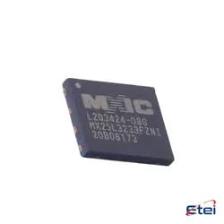
圖片僅供參考
TLV3401IDBVR
+物料清單IC OUT COMPARATR NANOPWR SOT23-5
-
製造商德州儀器
-
製造商部分 #TLV3401IDBVR
-
有存貨5497
365 天品質保證
7*24 小時服務保證
90-日售後保障
正品保證
規格
| 屬性 | 價值 |
| Package | Tape & Reel (TR),Cut Tape (CT),Bulk |
| ProductStatus | Active |
| Type | General Purpose |
| NumberofElements | 1 |
| OutputType | CMOS, Open-Drain |
| Voltage-SupplySingle/Dual(±) | 2.7V ~ 16V, ±1.35V ~ 8V |
| Voltage-InputOffset(Max) | 3.6mV @ 15V |
| Current-InputBias(Max) | 250pA @ 15V |
| Current-Output(Typ) | 10mA |
| Current-Quiescent(Max) | 950nA |
| CMRRPSRR(Typ) | 88dB CMRR, 105dB PSRR |
| PropagationDelay(Max) | 300µs |
| OperatingTemperature | -40°C ~ 125°C |
| Package/Case | SC-74A, SOT-753 |
| MountingType | Surface Mount |
概述
Description
The TLV3401IDBVR is a micropower, low-voltage comparator from Texas Instruments. It is designed for applications requiring low power consumption, operating with a supply voltage as low as 1.8V and consuming minimal quiescent current, typically around 2.8 µA. This makes it suitable for battery-powered devices and energy-efficient applications. The device offers a push-pull output stage, allowing it to source and sink current, thus facilitating direct interfacing with logic circuits.
The TLV3401IDBVR features a small signal bandwidth and operates efficiently at low frequencies. It has a wide input common-mode voltage range, extending from the negative supply rail to the positive supply minus 1.5V, which enhances its versatility in various signal conditions. The compact SOT-23 package makes it ideal for space-constrained applications.
Key applications include signal detection, voltage monitoring, and level shifting in consumer electronics, portable medical devices, and industrial controls. Its combination of low power, flexibility, and compact form factor makes the TLV3401IDBVR a reliable choice for modern electronic designs.
The TLV3401IDBVR features a small signal bandwidth and operates efficiently at low frequencies. It has a wide input common-mode voltage range, extending from the negative supply rail to the positive supply minus 1.5V, which enhances its versatility in various signal conditions. The compact SOT-23 package makes it ideal for space-constrained applications.
Key applications include signal detection, voltage monitoring, and level shifting in consumer electronics, portable medical devices, and industrial controls. Its combination of low power, flexibility, and compact form factor makes the TLV3401IDBVR a reliable choice for modern electronic designs.
Equivalent
The TLV3401IDBVR is a single-channel, nanopower, push-pull output comparator. Equivalent products from other manufacturers include the LMV721 from Texas Instruments, the MAX9025 from Maxim Integrated, and the MCP6541 from Microchip Technology. When selecting an equivalent, ensure compatibility in terms of voltage range, current consumption, response time, and package type to meet your specific application requirements.
Features
The TLV3401IDBVR is a single-channel, open-drain output comparator from Texas Instruments. It operates on a low voltage range from 2.7V to 16V, making it suitable for battery-powered applications. The device is designed for low power consumption, featuring a typical quiescent current of 4 µA, which helps extend battery life. With a fast response time, the TLV3401IDBVR has a typical propagation delay of 650 ns, enabling quick signal processing.
This comparator's open-drain output allows for easy interfacing with logic circuits and the ability to wire-OR multiple outputs. It features a wide input common-mode voltage range that extends below the negative supply rail, facilitating flexibility in various applications. The device is available in a small SOT-23 package, ideal for space-constrained designs. Its ambient temperature range of -40°C to 125°C ensures reliable operation in harsh environments. Overall, the TLV3401IDBVR is well-suited for portable electronics, consumer devices, and other applications requiring efficient and compact analog signal processing.
This comparator's open-drain output allows for easy interfacing with logic circuits and the ability to wire-OR multiple outputs. It features a wide input common-mode voltage range that extends below the negative supply rail, facilitating flexibility in various applications. The device is available in a small SOT-23 package, ideal for space-constrained designs. Its ambient temperature range of -40°C to 125°C ensures reliable operation in harsh environments. Overall, the TLV3401IDBVR is well-suited for portable electronics, consumer devices, and other applications requiring efficient and compact analog signal processing.
Pinout
The TLV3401IDBVR is a single-channel, low-voltage, nanopower comparator integrated circuit produced by Texas Instruments. It is available in a 5-pin SOT-23 package. Here are the pin details and functions:
1. V+ (Pin 5): This is the positive power supply pin. It provides the voltage supply to the device.
2. GND (Pin 2): Ground pin. It is connected to the ground of the power supply.
3. IN+ (Pin 3): Non-inverting input. The voltage applied here is compared to the voltage at the inverting input.
4. IN- (Pin 4): Inverting input. This is the reference voltage input for the comparator.
5. OUT (Pin 1): Output pin. The result of the comparison between the IN+ and IN- inputs is reflected here, typically as a high or low digital signal.
The TLV3401IDBVR is designed for ultra-low voltage and low-power applications, providing precise voltage comparison with minimal power consumption.
1. V+ (Pin 5): This is the positive power supply pin. It provides the voltage supply to the device.
2. GND (Pin 2): Ground pin. It is connected to the ground of the power supply.
3. IN+ (Pin 3): Non-inverting input. The voltage applied here is compared to the voltage at the inverting input.
4. IN- (Pin 4): Inverting input. This is the reference voltage input for the comparator.
5. OUT (Pin 1): Output pin. The result of the comparison between the IN+ and IN- inputs is reflected here, typically as a high or low digital signal.
The TLV3401IDBVR is designed for ultra-low voltage and low-power applications, providing precise voltage comparison with minimal power consumption.
Manufacturer
The TLV3401IDBVR is manufactured by Texas Instruments (TI). Texas Instruments is a global semiconductor company that designs and produces a wide range of electronic components, including integrated circuits, microcontrollers, and other semiconductor devices. TI is known for its innovation in analog and embedded processing products, serving industries such as consumer electronics, automotive, industrial, communications, and computing. The company focuses on developing technologies that facilitate efficient power management and enable high-performance electronics.
Application
The TLV3401IDBVR is an ultra-low-power comparator suitable for battery-powered and portable applications. Its application areas include:
1. Battery Monitoring: It can be used to monitor battery levels in portable devices.
2. Consumer Electronics: Useful for power management in devices such as smartphones and wearables.
3. Medical Devices: Ideal for low-power medical devices that require reliable signal processing.
4. Industrial Automation: Employed in systems needing efficient power management and low power consumption.
5. Power Management Systems: Suitable for overcurrent protection and voltage detection in power supplies.
6. Energy Harvesting: Used in systems that leverage low energy sources.
Its low supply current and wide voltage range make it versatile for various low-power applications.
1. Battery Monitoring: It can be used to monitor battery levels in portable devices.
2. Consumer Electronics: Useful for power management in devices such as smartphones and wearables.
3. Medical Devices: Ideal for low-power medical devices that require reliable signal processing.
4. Industrial Automation: Employed in systems needing efficient power management and low power consumption.
5. Power Management Systems: Suitable for overcurrent protection and voltage detection in power supplies.
6. Energy Harvesting: Used in systems that leverage low energy sources.
Its low supply current and wide voltage range make it versatile for various low-power applications.
Package
The TLV3401IDBVR is packaged in a SOT-23-5 (Small Outline Transistor) package. This package type is a small, surface-mount, five-pin configuration commonly used for space-efficient applications on printed circuit boards.