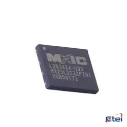
圖片僅供參考
SN74S10
+物料清單74S10 - TRIPLE 3-INPUT POSITIVE-
-
製造商德州儀器
-
製造商部分 #SN74S10
-
有存貨2086
365 天品質保證
7*24 小時服務保證
90-日售後保障
正品保證
規格
| 屬性 | 價值 |
| Package / Case | Bulk |
| Part Status | Active |
概述
Description
The SN74S10 is a digital logic integrated circuit from Texas Instruments, part of their 7400 series. It features three triple-input NAND gates. NAND gates are fundamental components in digital electronics, executing the logic operation where the output is false only if all the inputs are true. If one or more inputs are false, the output is true.
The SN74S10 is built using Schottky TTL (Transistor-Transistor Logic) technology, which offers faster switching speeds compared to standard TTL devices. This makes it suitable for high-speed applications. Schottky TTL achieves this by incorporating a Schottky diode to prevent the transistor from saturating, reducing the storage time and speeding up the operation.
Common applications for the SN74S10 include use in digital systems that require simple logic operations, such as microprocessors, memory address decoding, and other logic functions. It operates typically at a 5V supply and is known for its reliability and robustness in various applications. The chip is encapsulated in a 14-pin dual in-line package (DIP) or other surface-mount packages for different applications.
The SN74S10 is built using Schottky TTL (Transistor-Transistor Logic) technology, which offers faster switching speeds compared to standard TTL devices. This makes it suitable for high-speed applications. Schottky TTL achieves this by incorporating a Schottky diode to prevent the transistor from saturating, reducing the storage time and speeding up the operation.
Common applications for the SN74S10 include use in digital systems that require simple logic operations, such as microprocessors, memory address decoding, and other logic functions. It operates typically at a 5V supply and is known for its reliability and robustness in various applications. The chip is encapsulated in a 14-pin dual in-line package (DIP) or other surface-mount packages for different applications.
Equivalent
The SN74S10 is a triple 3-input NAND gate IC from the 7400 series TTL logic family. Equivalent products include the 74LS10, 74HC10, and 74HCT10, which are also triple 3-input NAND gates but with different characteristics regarding speed, power consumption, and technology. The 74LS series is Low-Power Schottky, while the 74HC and 74HCT are CMOS technology, offering lower power consumption. Compatibility should be checked based on the specific requirements of speed, voltage, and current.
Features
The SN74S10 is a triple 3-input NAND gate integrated circuit known for its high-speed operation and low power consumption. Key features include:
1. Logic Type: NAND Gate.
2. Number of Gates: It contains three separate 3-input NAND gates.
3. Input and Output: Standard TTL (Transistor-Transistor Logic) compatible inputs and outputs.
4. Propagation Delay: Typically around 4 ns, ensuring fast switching times.
5. Operating Voltage: Typically operates at a 5V power supply.
6. Current Consumption: Designed for low power usage, approximately 20 mA per gate.
7. Temperature Range: Functionality over a broad range of temperatures, usually 0°C to 70°C.
8. Package Type: Available in a 14-pin DIP (Dual In-line Package).
9. Fan-out: Can drive up to 10 standard TTL loads.
10. Noise Margin: Provides adequate noise margin for reliable operation.
These features make the SN74S10 suitable for a variety of digital logic applications where speed and efficiency are crucial.
1. Logic Type: NAND Gate.
2. Number of Gates: It contains three separate 3-input NAND gates.
3. Input and Output: Standard TTL (Transistor-Transistor Logic) compatible inputs and outputs.
4. Propagation Delay: Typically around 4 ns, ensuring fast switching times.
5. Operating Voltage: Typically operates at a 5V power supply.
6. Current Consumption: Designed for low power usage, approximately 20 mA per gate.
7. Temperature Range: Functionality over a broad range of temperatures, usually 0°C to 70°C.
8. Package Type: Available in a 14-pin DIP (Dual In-line Package).
9. Fan-out: Can drive up to 10 standard TTL loads.
10. Noise Margin: Provides adequate noise margin for reliable operation.
These features make the SN74S10 suitable for a variety of digital logic applications where speed and efficiency are crucial.
Pinout
The SN74S10 is a triple 3-input NAND gate IC from the 74S series, which is a TTL (Transistor-Transistor Logic) family known for its speed. This IC features three separate NAND gates, each with three inputs.
The SN74S10 comes in a 14-pin Dual Inline Package (DIP). The pin configuration is as follows:
- Pins 1, 2, 13: Inputs for the first NAND gate.
- Pin 12: Output for the first NAND gate.
- Pins 3, 4, 5: Inputs for the second NAND gate.
- Pin 6: Output for the second NAND gate.
- Pins 8, 9, 10: Inputs for the third NAND gate.
- Pin 11: Output for the third NAND gate.
- Pin 7: Ground (GND) connection.
- Pin 14: Positive supply voltage (Vcc).
The primary function of the SN74S10 is to perform the logical NAND operation on three input signals per gate, providing flexibility in digital circuit design.
The SN74S10 comes in a 14-pin Dual Inline Package (DIP). The pin configuration is as follows:
- Pins 1, 2, 13: Inputs for the first NAND gate.
- Pin 12: Output for the first NAND gate.
- Pins 3, 4, 5: Inputs for the second NAND gate.
- Pin 6: Output for the second NAND gate.
- Pins 8, 9, 10: Inputs for the third NAND gate.
- Pin 11: Output for the third NAND gate.
- Pin 7: Ground (GND) connection.
- Pin 14: Positive supply voltage (Vcc).
The primary function of the SN74S10 is to perform the logical NAND operation on three input signals per gate, providing flexibility in digital circuit design.
Manufacturer
The SN74S10 is manufactured by Texas Instruments (TI). Texas Instruments is an American technology company that designs and manufactures semiconductors and various integrated circuits, which are used in electronic devices globally. TI is one of the largest producers of analog technology components and is also a leading supplier of digital signal processors and microcontrollers. The company serves a broad range of industries, including automotive, industrial, personal electronics, and communications equipment. TI is renowned for its innovation in the field of electronics and its emphasis on research and development to advance semiconductor technology.
Application
The SN74S10 is a triple 3-input NAND gate integrated circuit used in digital electronics. Its application areas include:
1. Digital Logic Design: Utilized to implement basic logic functions and complex gate networks.
2. Signal Processing: Used in creating combinational logic systems for signal modification.
3. Computing Systems: Integral in building microprocessor and microcontroller circuits.
4. Industrial Control Systems: Employed in automation for processing control logic.
5. Telecommunications: Used in data routing and switching systems.
6. Consumer Electronics: Forms part of digital circuits in gadgets and appliances.
7. Educational Purposes: Often used in teaching and prototyping digital circuits due to its basic logic functionality.
These applications benefit from the chip's high-speed performance and reliability.
1. Digital Logic Design: Utilized to implement basic logic functions and complex gate networks.
2. Signal Processing: Used in creating combinational logic systems for signal modification.
3. Computing Systems: Integral in building microprocessor and microcontroller circuits.
4. Industrial Control Systems: Employed in automation for processing control logic.
5. Telecommunications: Used in data routing and switching systems.
6. Consumer Electronics: Forms part of digital circuits in gadgets and appliances.
7. Educational Purposes: Often used in teaching and prototyping digital circuits due to its basic logic functionality.
These applications benefit from the chip's high-speed performance and reliability.
Package
The SN74S10 is a TTL logic IC featuring three 3-input NAND gates. It is typically available in dual in-line package (DIP) and small outline integrated circuit (SOIC) package types, suitable for through-hole and surface-mount applications, respectively.