
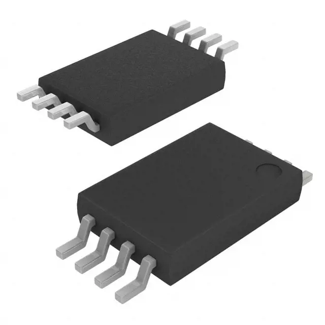
圖片僅供參考
NB3V1104CDTR2G
+物料清單IC CLK BUFFER 1:4 250MHZ 8TSSOP
-
製造商安森美
-
製造商部分 #NB3V1104CDTR2G
-
有存貨4419
365 天品質保證
7*24 小時服務保證
90-日售後保障
正品保證
規格
| 屬性 | 價值 |
| Part Status | Active |
| Type | Fanout Buffer (Distribution) |
| Number of Circuits | 1 |
| Ratio - Input: Output | 1:4 |
| Differential - Input: Output | No/No |
| Input | LVCMOS |
| Output | LVCMOS |
| Frequency - Max | 250 MHz |
| Voltage - Supply | 1.71V ~ 3.6V |
| Operating Temperature | -40°C ~ 105°C |
| Mounting Type | Surface Mount |
| Package / Case | 8-TSSOP (0.173", 4.40mm Width) |
| Supplier Device Package | 8-TSSOP |
| Base Product Number | NB3V1104 |
概述
Description
The NB3V1104CDTR2G is a high-performance voltage-level translator designed for communication between different voltage domains, typically used in digital applications. It enables bidirectional data transfer between devices operating at different supply voltages, making it suitable for interfacing 1.2V, 1.5V, 1.8V, 2.5V, and 3.3V logic levels.
Key features include low propagation delay, low power consumption, and robust ESD protection, enhancing device reliability. The NB3V1104CDTR2G supports multiple channels (typically four), allowing for simultaneous communication paths, which is advantageous in complex systems. Its small package size (usually offered in a compact QFN or SOIC) simplifies integration into various circuit designs.
This device is commonly used in applications such as mobile devices, automotive electronics, and any system requiring logic level shifting between components with varying voltage requirements. Overall, the NB3V1104CDTR2G is essential for ensuring interoperability in mixed-voltage environments.
Key features include low propagation delay, low power consumption, and robust ESD protection, enhancing device reliability. The NB3V1104CDTR2G supports multiple channels (typically four), allowing for simultaneous communication paths, which is advantageous in complex systems. Its small package size (usually offered in a compact QFN or SOIC) simplifies integration into various circuit designs.
This device is commonly used in applications such as mobile devices, automotive electronics, and any system requiring logic level shifting between components with varying voltage requirements. Overall, the NB3V1104CDTR2G is essential for ensuring interoperability in mixed-voltage environments.
Equivalent
The NB3V1104CDTR2G is a low-skew clock buffer. Equivalent products include the IDT 5P49V5920, MAXIM MAX5080, and the NXP 74LVC1G94. Always verify specific electrical characteristics and application suitability when selecting alternatives.
Features
The NB3V1104CDTR2G is a high-performance, low-jitter, clock buffer designed for various applications. Key features include:
1. Input and Output: It supports a single input and four outputs, allowing for distribution of a clock signal to multiple destinations.
2. Low Jitter: The device offers low phase jitter, enhancing signal integrity in high-speed applications.
3. Wide Voltage Range: Operates with a power supply range of 2.5V to 3.6V, making it versatile for different systems.
4. Compatibility: Compatible with various logic families, including LVPECL, LVDS, and CMOS.
5. Temperature Range: Designed for reliable operation over an industrial temperature range of -40°C to +85°C.
6. Low Power Consumption: Optimized for efficiency, making it suitable for power-sensitive applications.
7. Easy Integration: Small package size (TSSOP) facilitates integration into compact designs.
Overall, the NB3V1104CDTR2G is ideal for communication systems, data centers, and consumer electronics requiring efficient clock distribution.
1. Input and Output: It supports a single input and four outputs, allowing for distribution of a clock signal to multiple destinations.
2. Low Jitter: The device offers low phase jitter, enhancing signal integrity in high-speed applications.
3. Wide Voltage Range: Operates with a power supply range of 2.5V to 3.6V, making it versatile for different systems.
4. Compatibility: Compatible with various logic families, including LVPECL, LVDS, and CMOS.
5. Temperature Range: Designed for reliable operation over an industrial temperature range of -40°C to +85°C.
6. Low Power Consumption: Optimized for efficiency, making it suitable for power-sensitive applications.
7. Easy Integration: Small package size (TSSOP) facilitates integration into compact designs.
Overall, the NB3V1104CDTR2G is ideal for communication systems, data centers, and consumer electronics requiring efficient clock distribution.
Pinout
The NB3V1104CDTR2G is a quad 2:1 multiplexer designed for signal routing in high-speed applications. It features a 16-pin TSSOP (Thin Shrink Small Outline Package) form factor. The pin count is 16.
Key functions include:
- Four independent 2:1 multiplexers, allowing selection between two inputs for each channel.
- It operates with a supply voltage range of 3V to 3.6V, making it suitable for low-voltage applications.
- The device is designed for high-speed performance, supporting data rates up to 1.5 GHz.
- It includes enable pins to control the operation of the multiplexers, providing flexibility in signal routing.
The NB3V1104CDTR2G is commonly used in applications such as data routing, clock switching, and signal multiplexing in communication systems.
Key functions include:
- Four independent 2:1 multiplexers, allowing selection between two inputs for each channel.
- It operates with a supply voltage range of 3V to 3.6V, making it suitable for low-voltage applications.
- The device is designed for high-speed performance, supporting data rates up to 1.5 GHz.
- It includes enable pins to control the operation of the multiplexers, providing flexibility in signal routing.
The NB3V1104CDTR2G is commonly used in applications such as data routing, clock switching, and signal multiplexing in communication systems.
Manufacturer
The NB3V1104CDTR2G is manufactured by ON Semiconductor, a global supplier of semiconductor-based solutions. ON Semiconductor designs, manufactures, and sells a wide range of products, including analog, digital, and mixed-signal integrated circuits, as well as discrete components. The company serves various industries, including automotive, industrial, cloud, and consumer electronics.
Founded in 1999, ON Semiconductor has grown through both organic development and strategic acquisitions, expanding its portfolio and market presence. The company's focus is on providing energy-efficient solutions and enabling the development of advanced technologies, including those related to IoT, automotive safety, and power management.
ON Semiconductor's commitment to innovation and quality has made it a key player in the semiconductor industry, catering to a diverse set of applications and customer needs.
Founded in 1999, ON Semiconductor has grown through both organic development and strategic acquisitions, expanding its portfolio and market presence. The company's focus is on providing energy-efficient solutions and enabling the development of advanced technologies, including those related to IoT, automotive safety, and power management.
ON Semiconductor's commitment to innovation and quality has made it a key player in the semiconductor industry, catering to a diverse set of applications and customer needs.
Application
The NB3V1104CDTR2G is a high-performance clock buffer and fanout driver used in various applications, including high-speed data communication systems, telecommunications, and networking equipment. It is ideal for distributing clock signals in data converters, FPGAs, and microprocessors. Additionally, it supports video applications where precise timing is critical, making it suitable for use in video processing and transmission systems. Its ability to drive multiple loads while maintaining signal integrity makes it valuable in complex electronic systems requiring robust clock management.
Package
The NB3V1104CDTR2G is packaged in a 16-pin TSSOP (Thin Shrink Small Outline Package). This compact package type is designed for efficient space utilization on PCBs.


