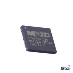
圖片僅供參考
N25Q512A13GSFA0F
+物料清單NOR Flash SPI 512Mbit 4 16/16 SOIC 2 UT
-
製造商微米
-
製造商部分 #N25Q512A13GSFA0F
-
有存貨25985
365 天品質保證
7*24 小時服務保證
90-日售後保障
正品保證
規格
| 屬性 | 價值 |
| Packaging | MouseReel |
| Standard Pack Qty | 1000 |
概述
Description
The N25Q512A13GSFA0F is a high-performance, non-volatile NOR Flash memory device manufactured by Micron Technology. It is part of the N25Q series, known for offering reliable storage solutions suitable for embedded systems and other applications requiring robust data retention and fast access speeds. This specific model is characterized by its 512 Mb (megabit) memory capacity, making it suitable for use in various applications that require moderate storage space.
The device features a Serial Peripheral Interface (SPI), which facilitates easy integration with microcontrollers and other digital devices. It supports multiple I/O configurations, including single, dual, and quad I/O, which allow for flexible communication and faster data transfers. The N25Q512A13GSFA0F operates at a wide voltage range, typically from 2.7V to 3.6V, making it versatile for different power conditions.
The N25Q512A13GSFA0F is designed to withstand harsh environments, offering reliable performance over a wide temperature range. This makes it ideal for use in industrial, automotive, and consumer electronics applications.
The device features a Serial Peripheral Interface (SPI), which facilitates easy integration with microcontrollers and other digital devices. It supports multiple I/O configurations, including single, dual, and quad I/O, which allow for flexible communication and faster data transfers. The N25Q512A13GSFA0F operates at a wide voltage range, typically from 2.7V to 3.6V, making it versatile for different power conditions.
The N25Q512A13GSFA0F is designed to withstand harsh environments, offering reliable performance over a wide temperature range. This makes it ideal for use in industrial, automotive, and consumer electronics applications.
Equivalent
The N25Q512A13GSFA0F is a 512 Mbit serial NOR flash memory chip from Micron. Equivalent products could include similar Flash memory chips from manufacturers like Winbond (e.g., W25Q512JV), Microchip (e.g., AT25DF641A), and Macronix (e.g., MX25L51245G). It is important to verify compatibility based on specifications such as memory size, interface type, voltage requirements, and operating temperature range. Always refer to datasheets for precise equivalency.
Features
The N25Q512A13GSFA0F is a 512 Mbit (64 MB) serial NOR Flash memory device from Micron Technology. Key features include:
1. Memory Architecture: Organized in a 65,536-by-64-byte page structure, enabling efficient data storage and retrieval.
2. Interface: Utilizes a Serial Peripheral Interface (SPI) for high-speed data transfer, supporting single, dual, and quad I/O operations for enhanced flexibility.
3. Performance: Offers fast read speeds up to 108 MHz in extended SPI mode and supports double data rate (DDR) operations to improve throughput.
4. Data Protection: Includes security features such as block protection, password protection, and a one-time programmable (OTP) area for secure data storage.
5. Endurance and Retention: Provides reliable endurance with up to 100,000 program/erase cycles per sector and data retention of 20 years.
6. Operating Voltage: Operates at a wide voltage range of 2.7V to 3.6V, suitable for various applications.
7. Package: Available in a compact WSON-8 package to accommodate space constraints in embedded systems.
These features make it suitable for use in consumer electronics, industrial applications, and other devices requiring reliable non-volatile memory storage.
1. Memory Architecture: Organized in a 65,536-by-64-byte page structure, enabling efficient data storage and retrieval.
2. Interface: Utilizes a Serial Peripheral Interface (SPI) for high-speed data transfer, supporting single, dual, and quad I/O operations for enhanced flexibility.
3. Performance: Offers fast read speeds up to 108 MHz in extended SPI mode and supports double data rate (DDR) operations to improve throughput.
4. Data Protection: Includes security features such as block protection, password protection, and a one-time programmable (OTP) area for secure data storage.
5. Endurance and Retention: Provides reliable endurance with up to 100,000 program/erase cycles per sector and data retention of 20 years.
6. Operating Voltage: Operates at a wide voltage range of 2.7V to 3.6V, suitable for various applications.
7. Package: Available in a compact WSON-8 package to accommodate space constraints in embedded systems.
These features make it suitable for use in consumer electronics, industrial applications, and other devices requiring reliable non-volatile memory storage.
Pinout
The N25Q512A13GSFA0F is a 512 Mbit (64 MB) serial Flash memory device manufactured by Micron Technology. It features a total of 8 pins, which are commonly used in such NOR Flash memory devices. The pin functions are as follows:
1. CS# (Chip Select): Enables the device, active low.
2. SCK (Serial Clock): Provides the clock signal to synchronize data transfer.
3. DQ0 (Data Input/Output 0): Serves as a data line for input or output.
4. DQ1 (Data Input/Output 1): Serves as a data line for input or output.
5. DQ2 (Data Input/Output 2): Serves as a data line for input or output.
6. DQ3 (Data Input/Output 3): Serves as a data line for input or output.
7. VCC (Supply Voltage): Provides the power supply to the device.
8. VSS (Ground): Ground reference for the power supply.
These pins work together to manage the read, write, and erase operations of the memory, supporting a variety of protocols including SPI and Dual/Quad I/O SPI.
1. CS# (Chip Select): Enables the device, active low.
2. SCK (Serial Clock): Provides the clock signal to synchronize data transfer.
3. DQ0 (Data Input/Output 0): Serves as a data line for input or output.
4. DQ1 (Data Input/Output 1): Serves as a data line for input or output.
5. DQ2 (Data Input/Output 2): Serves as a data line for input or output.
6. DQ3 (Data Input/Output 3): Serves as a data line for input or output.
7. VCC (Supply Voltage): Provides the power supply to the device.
8. VSS (Ground): Ground reference for the power supply.
These pins work together to manage the read, write, and erase operations of the memory, supporting a variety of protocols including SPI and Dual/Quad I/O SPI.
Manufacturer
The N25Q512A13GSFA0F is a serial flash memory chip manufactured by Micron Technology, Inc. Micron is a leading global company specializing in the production of semiconductor devices, primarily memory and storage solutions. The company is a major player in the technology industry, providing products like DRAM, NAND, and NOR flash memory, which are crucial components in a wide range of electronic devices, from personal computers and mobile devices to data centers and automotive systems. Micron's products are integral to advancements in technology such as artificial intelligence, machine learning, and the Internet of Things (IoT), reflecting its role in driving innovation and supporting the infrastructure of modern computing environments.
Application
The N25Q512A13GSFA0F is a 512Mb serial NOR Flash memory chip commonly used in applications requiring reliable, non-volatile storage. Its primary application areas include:
1. Embedded Systems: Provides firmware storage for microcontrollers and microprocessors in various electronic devices.
2. Consumer Electronics: Used in devices like smart TVs, set-top boxes, and wearable technology for boot code and data storage.
3. Industrial Automation: Supports data logging and configuration storage in machinery and equipment.
4. Automotive: Stores firmware and calibration data for infotainment systems and electronic control units (ECUs).
5. Networking Equipment: Utilized in routers and switches for firmware and configuration data storage.
The chip's high-speed SPI interface and uniform sector architecture make it suitable for these applications.
1. Embedded Systems: Provides firmware storage for microcontrollers and microprocessors in various electronic devices.
2. Consumer Electronics: Used in devices like smart TVs, set-top boxes, and wearable technology for boot code and data storage.
3. Industrial Automation: Supports data logging and configuration storage in machinery and equipment.
4. Automotive: Stores firmware and calibration data for infotainment systems and electronic control units (ECUs).
5. Networking Equipment: Utilized in routers and switches for firmware and configuration data storage.
The chip's high-speed SPI interface and uniform sector architecture make it suitable for these applications.
Package
The N25Q512A13GSFA0F is a flash memory device packaged in a 24-ball TBGA (Thin Ball Grid Array) format.