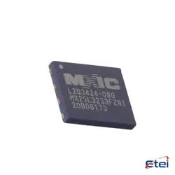
圖片僅供參考
MX29LV040CQI-70G
+物料清單IC FLASH 4MBIT PARALLEL 32PLCC
-
製造商旺宏
-
製造商部分 #MX29LV040CQI-70G
-
有存貨2074
365 天品質保證
7*24 小時服務保證
90-日售後保障
正品保證
規格
| 屬性 | 價值 |
| Series | MX29LV |
| Part Status | Obsolete |
| Base Product Number | MX29LV040 |
| DigiKey Programmable | Not Verified |
| Memory Type | Non-Volatile |
| Memory Format | FLASH |
| Technology | FLASH - NOR |
| Memory Size | 4Mbit |
| Memory Organization | 512K x 8 |
| Memory Interface | Parallel |
| Write Cycle Time - Word, Page | 70ns |
| Voltage - Supply | 2.7V ~ 3.6V |
| Operating Temperature | -40°C ~ 85°C (TA) |
| Mounting Type | Surface Mount |
| Package | 32-LCC (J-Lead) |
| Supplier Device Package | 32-PLCC (11.43x14.05) |
| Packaging | Tray |
| Access Time | 70 ns |
概述
Description
The chip is designed to be used in a range of consumer electronics, embedded systems, and industrial applications due to its reliable non-volatile storage capabilities. It supports a standard parallel NOR flash interface, allowing for ease of integration into existing systems. The MX29LV040CQI-70G is also equipped with additional functions such as sector erase and byte program capabilities, enhancing its flexibility in data management.
Furthermore, it comes in a compact package, suitable for space-constrained environments. The chip's endurance and data retention capabilities ensure long-term reliability, making it a popular choice for developers seeking efficient and durable memory solutions.
Equivalent
1. SST39SF040 - by Microchip Technology
2. AT29C040A - by Atmel (now Microchip Technology)
3. AM29F040B - by AMD (Spansion/Cypress)
4. W29C040-90 - by Winbond
These alternatives offer similar storage capacities and functionalities, but variations in timing, voltage, and package types should be considered for compatibility. Always verify specifications to ensure they meet your specific requirements.
Features
1. Density and Organization: It offers a 4 Mbit density organized as 512K x 8 bits.
2. Sector Architecture: The memory contains 8 sectors, enabling flexible erase capabilities.
3. Read Speed: It features a fast read performance with an access time of 70 ns.
4. Voltage Range: The chip operates within a 2.7V to 3.6V range, making it suitable for low-voltage applications.
5. Endurance: Each sector can endure up to 100,000 program/erase cycles.
6. Data Retention: It provides data retention of more than 10 years.
7. Low Power Consumption: Supports standby and automatic power-down modes for reduced power usage.
8. Packaging: Available in a 32-pin PLCC package.
9. Interfaces: Features a standard parallel interface for easy integration.
10. Temperature Range: Industrial temperature range, typically -40°C to 85°C.
These features make it suitable for applications requiring reliable and high-density non-volatile memory.
Pinout
1. Pin Count: 32 pins.
2. Architecture: Organized as 512K x 8 bits.
3. Voltage Supply: Operates on a single 3.0-3.6V power supply.
4. Speed: 70 ns access time.
5. Memory Organization: Divided into uniform sectors for erase functionality.
6. Write and Erase: Allows for byte-level programming and sector/chip erase operations.
7. Endurance: High endurance with typical 100,000 program/erase cycles per sector.
8. Data Retention: Offers data retention of at least 10 years.
These features make the MX29LV040CQI-70G suitable for a wide range of applications requiring reliable and non-volatile storage solutions.
Manufacturer
Application
1. Embedded Systems: Provides firmware storage for microcontrollers and microprocessors.
2. Consumer Electronics: Used in devices like digital cameras, gaming consoles, and set-top boxes for program and data storage.
3. Industrial Equipment: Stores configuration data and system firmware for robustness in control systems.
4. Networking Devices: Utilized in routers and switches for storing firmware and configuration data.
5. Automotive Systems: Retains critical software for infotainment systems and electronic control units (ECUs).
Its low power consumption and wide temperature range make it suitable for various applications requiring reliable flash memory.
Package
Frequently Asked Questions
Q: What is the memory size and organization of the MX29LV040CQI-70G?
A: It has a 4Mbit capacity organized as 512K x 8 bits, ideal for firmware storage.
Q: What is the access time and voltage range for this device?
A: Access time is 70 ns, and the supply voltage range is 2.7V to 3.6V, ensuring fast reads in low-power designs.
Q: Is this component suitable for industrial temperature applications?
A: Yes, it operates from -40°C to 85°C, making it reliable for harsh environments.
Q: What memory interface and packaging type does it use?
A: It uses a parallel memory interface and comes in a 32-PLCC (J-Lead) surface-mount package.
Q: Is this NOR Flash memory programmable for code or data storage?
A: Yes, it is a NOR Flash, with a write cycle time of 70ns per word/page, suitable for code execution and data retention.
Q: Does this part support standard programming algorithms or require special commands?
A: It follows standard parallel NOR Flash programming protocols, compatible with typical microcontroller and FPGA interfaces.