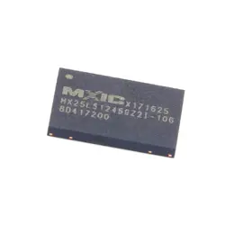
規格
| 屬性 | 價值 |
| Brand | Micron |
| Mounting Type | SMD/SMT |
| Product Type | DRAM |
| Subcategory | Memory & Data Storage |
| Minimum Operating Temperature | 0 C |
| Maximum Operating Temperature | + 70 C |
| Series | MT48LC |
| Supply Voltage - Min | 3 V |
| Supply Voltage - Max | 3.6 V |
| Package / Case | TSOP-54 |
| Current - Supply (Max) | 125 mA |
| Type | SDRAM |
| Data Bus Width | 16 bit |
| Maximum Clock Frequency | 133 MHz |
| Memory Size | 64 Mbit |
| Access Time | 5.4 ns |
| Organisation | 4 M x 16 |
概述
Description
This memory chip supports a low voltage of 1.8V, which is ideal for reducing power consumption in modern electronic systems. It is compatible with various memory standards and protocols, ensuring versatility in integration. The chip is typically packaged in a TSOP (Thin Small Outline Package), facilitating easy mounting on circuit boards.
Overall, the MT48LC4M16A2TG-7E is designed for high-performance applications, providing reliable and efficient memory solutions for a wide range of devices.
Equivalent
1. Hynix HY57V641620C
2. Micron MT48LC4M16A2P
3. Samsung K4S281632E
4. Nanya NT5CB256M8
5. Winbond W9751G6KB-25
Always verify compatibility with specific system requirements before replacement.
Features
1. Density: 64 Megabits, organized as 4 Megabytes x 16 bits.
2. Technology: DDR (Double Data Rate) SDRAM, enabling data transfer on both the rising and falling edges of the clock cycle.
3. Speed: Operates at a clock frequency of 133 MHz, with a data rate of 266 MT/s.
4. Voltage: Operates on a 2.5V power supply, with a low power consumption profile.
5. Latency: Supports various burst lengths (1, 2, 4, 8) and has improved latency characteristics for enhanced performance.
6. Packaging: Available in a standard 54-ball TSOP II package, suitable for various applications.
7. Applications: Ideal for use in consumer electronics, telecommunications, and networking equipment.
The MT48LC4M16A2TG-7E combines high performance, low power consumption, and reliable data integrity for diverse memory applications.
Pinout
The functions of the pins are as follows:
- Data Pins (DQ0-DQ15): 16 pins for data input/output.
- Address Pins (A0-A12): 13 pins for addressing memory locations.
- Control Pins:
- CAS (Column Address Strobe): Used to latch the column address.
- RAS (Row Address Strobe): Used to latch the row address.
- WE (Write Enable): Controls write operations.
- CS (Chip Select): Activates the chip for communication.
- Clock Pins (CLK, CLK): For synchronizing operations.
- Baud Rate Pins (BA0, BA1): Selects bank address.
- Other Pins:
- VDD/VSS: Power supply and ground connections.
- ODT (On-Die Termination): For impedance matching.
This chip is commonly used in various computing applications for memory storage.
Manufacturer
Application
Package
Frequently Asked Questions
Q: What is the memory organization of this Micron SDRAM?
A: It is organized as 4 M x 16 bits, providing a total memory size of 64 Mbit.
Q: Does this DRAM support a 133 MHz system clock?
A: Yes, it supports a maximum clock frequency of 133 MHz for standard SDRAM operations.
Q: What is the typical supply voltage range for this chip?
A: It operates with a supply voltage from 3.0 V (min) to 3.6 V (max).
Q: What is the access time for this MT48LC part?
A: The access time is 5.4 ns, suitable for high-speed data retrieval.
Q: What is the operating temperature range for this model?
A: Its commercial temperature range is from 0°C to +70°C.
Q: What is the maximum supply current consumption?
A: The maximum supply current is 125 mA under specified operating conditions.
Q: In which package is this SDRAM available?
A: It is housed in a standard TSOP-54 (Thin Small Outline Package) for SMD/SMT mounting.