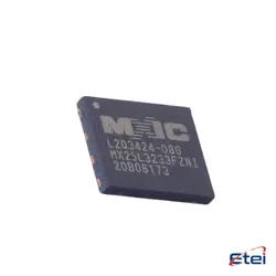
圖片僅供參考
MT48LC32M16A2P-75 IT:C
+物料清單3V~3.6V 512Mbit 133MHz 54-TSOP II Memory (ICs)
-
製造商微米
-
製造商部分 #MT48LC32M16A2P-75 IT:C
-
有存貨5147
365 天品質保證
7*24 小時服務保證
90-日售後保障
正品保證
規格
| 屬性 | 價值 |
| Packaging | 54-TSOP II |
| Clock Frequency | 133MHz |
| Memory Size | 512Mbit |
| Operating Temperature | -40℃~+85℃ |
| Voltage - Supply | 3V~3.6V |
概述
Description
The MT48LC32M16A2P-75 IT:C is a 512Mb SDRAM (Synchronous Dynamic Random-Access Memory) chip designed by Micron Technology. It features a memory configuration of 32M x 16 bits and operates with a clock frequency of up to 133 MHz. The chip uses a 3.3V power supply and supports CAS (Column Address Strobe) latencies of 2 and 3. It is organized as four banks of 8M words, each with a refresh period of 64ms.
This SDRAM is ideal for applications requiring high-performance memory, such as computing and graphics. It supports burst lengths of 1, 2, 4, 8, and a full page, allowing for flexible data access patterns. The "-75 IT:C" suffix denotes a speed grade of 7.5ns and industrial temperature range (-40°C to 85°C), making it suitable for use in various environmental conditions.
The MT48LC32M16A2P-75 IT:C offers efficient data management and high-speed data transfer, contributing to improved system performance. It is commonly used in systems where reliable and fast memory access is critical.
This SDRAM is ideal for applications requiring high-performance memory, such as computing and graphics. It supports burst lengths of 1, 2, 4, 8, and a full page, allowing for flexible data access patterns. The "-75 IT:C" suffix denotes a speed grade of 7.5ns and industrial temperature range (-40°C to 85°C), making it suitable for use in various environmental conditions.
The MT48LC32M16A2P-75 IT:C offers efficient data management and high-speed data transfer, contributing to improved system performance. It is commonly used in systems where reliable and fast memory access is critical.
Equivalent
The MT48LC32M16A2P-75 IT:C is a 512Mb SDRAM chip. Equivalent products can include:
1. Samsung K4S561632J
2. Hynix HY57V561620FTP-H
3. Nanya NT5DS32M16BG
4. Winbond W9825G6KH
These are similar in terms of memory capacity, speed, and configuration. Always check the specific datasheets for compatibility and other specifications before choosing a substitute.
1. Samsung K4S561632J
2. Hynix HY57V561620FTP-H
3. Nanya NT5DS32M16BG
4. Winbond W9825G6KH
These are similar in terms of memory capacity, speed, and configuration. Always check the specific datasheets for compatibility and other specifications before choosing a substitute.
Features
The MT48LC32M16A2P-75 IT:C is a 512 Mb SDRAM (Synchronous Dynamic Random-Access Memory) from Micron Technology. Key features include:
1. Density and Organization: It is organized as 32M x 16 and offers a 512 Megabit capacity.
2. Speed and Performance: The device has a clock rate of 133 MHz with a CAS latency of 3, enabling efficient data transfer.
3. Voltage: Operates at a voltage supply of 3.3V, which is standard for SDRAMs, ensuring compatibility with a wide range of systems.
4. Temperature Range: The device is designed for industrial temperature ranges, from -40°C to 85°C, making it suitable for demanding applications.
5. Package: Available in a 54-pin TSOP (Thin Small Outline Package) type II, which is space-efficient and suitable for compact designs.
6. Data Transfer: Supports burst lengths of 1, 2, 4, 8, and a full-page, allowing flexible data handling.
These features make the MT48LC32M16A2P-75 IT:C suitable for a variety of applications, including industrial, automotive, and networking equipment.
1. Density and Organization: It is organized as 32M x 16 and offers a 512 Megabit capacity.
2. Speed and Performance: The device has a clock rate of 133 MHz with a CAS latency of 3, enabling efficient data transfer.
3. Voltage: Operates at a voltage supply of 3.3V, which is standard for SDRAMs, ensuring compatibility with a wide range of systems.
4. Temperature Range: The device is designed for industrial temperature ranges, from -40°C to 85°C, making it suitable for demanding applications.
5. Package: Available in a 54-pin TSOP (Thin Small Outline Package) type II, which is space-efficient and suitable for compact designs.
6. Data Transfer: Supports burst lengths of 1, 2, 4, 8, and a full-page, allowing flexible data handling.
These features make the MT48LC32M16A2P-75 IT:C suitable for a variety of applications, including industrial, automotive, and networking equipment.
Pinout
The MT48LC32M16A2P-75 IT:C is a 512Mb SDRAM (Synchronous Dynamic Random-Access Memory) chip manufactured by Micron Technology. It is organized as 32M x 16 bits and comes in a 54-pin TSOP (Thin Small-Outline Package).
The primary functions of the pins include:
1. Data Pins (DQ0-DQ15): Used for data input/output.
2. Address Pins (A0-A12): Used to select the memory location.
3. Bank Address Pins (BA0, BA1): Used to select one of the four internal banks.
4. Control Pins:
- CLK: Clock input for synchronization.
- CKE: Clock Enable, to enable or disable the clock.
- CS#: Chip Select, to enable or disable the device.
- RAS#, CAS#, WE#: Row Address Strobe, Column Address Strobe, and Write Enable for controlling various operations.
5. Power Supply Pins (VDD, VSS): Power and ground connections.
6. DQS: Data strobe for data signal timing.
7. DM: Data mask for write operations.
This configuration allows for efficient memory management and high-speed data operations in various applications.
The primary functions of the pins include:
1. Data Pins (DQ0-DQ15): Used for data input/output.
2. Address Pins (A0-A12): Used to select the memory location.
3. Bank Address Pins (BA0, BA1): Used to select one of the four internal banks.
4. Control Pins:
- CLK: Clock input for synchronization.
- CKE: Clock Enable, to enable or disable the clock.
- CS#: Chip Select, to enable or disable the device.
- RAS#, CAS#, WE#: Row Address Strobe, Column Address Strobe, and Write Enable for controlling various operations.
5. Power Supply Pins (VDD, VSS): Power and ground connections.
6. DQS: Data strobe for data signal timing.
7. DM: Data mask for write operations.
This configuration allows for efficient memory management and high-speed data operations in various applications.
Manufacturer
The MT48LC32M16A2P-75 IT:C is a DRAM chip manufactured by Micron Technology, Inc. Micron is a leading global corporation in the semiconductor industry, specializing in the production of memory and storage solutions. The company produces a variety of memory technologies, including DRAM (Dynamic Random-Access Memory), NAND flash memory, and NOR flash memory, which are critical components in computers, consumer electronics, networking devices, and mobile devices. Founded in 1978 and headquartered in Boise, Idaho, USA, Micron has grown to become one of the world's largest memory manufacturers. Their products are used in a wide range of applications, from personal computing and mobile devices to automotive and industrial systems. Beyond manufacturing, Micron is also active in research and development, aiming to advance memory technologies and improve data storage capabilities.
Application
The MT48LC32M16A2P-75 IT:C is a 512 Mb SDRAM (Synchronous Dynamic Random-Access Memory) commonly used in various applications requiring quick data access and processing. Typical application areas include:
1. Embedded Systems: Utilized in automotive, industrial controls, and consumer electronics for efficient data handling.
2. Networking: Employed in routers, switches, and other network equipment for buffering and memory storage.
3. Telecommunications: Used in base stations and communication devices for data processing.
4. Computing: Integrated into PCs, laptops, and servers for memory tasks.
5. Consumer Electronics: Found in gaming consoles, digital cameras, and smart appliances for enhanced multimedia performance.
These applications benefit from its fast access time, reliability, and efficient performance.
1. Embedded Systems: Utilized in automotive, industrial controls, and consumer electronics for efficient data handling.
2. Networking: Employed in routers, switches, and other network equipment for buffering and memory storage.
3. Telecommunications: Used in base stations and communication devices for data processing.
4. Computing: Integrated into PCs, laptops, and servers for memory tasks.
5. Consumer Electronics: Found in gaming consoles, digital cameras, and smart appliances for enhanced multimedia performance.
These applications benefit from its fast access time, reliability, and efficient performance.
Package
The MT48LC32M16A2P-75 IT:C is a DRAM memory chip from Micron Technology, specifically a 512Mb SDRAM organized as 32M x 16. It is available in a 54-pin plastic Thin Small Outline Package (TSOP) Type II.