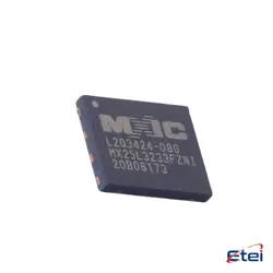
圖片僅供參考
MT48LC2M32B2P-6A:J
+物料清單IC DRAM 64MBIT PAR 86TSOP II
-
製造商美光科技股份有限公司。
-
製造商部分 #MT48LC2M32B2P-6A:J
-
有存貨2627
365 天品質保證
7*24 小時服務保證
90-日售後保障
正品保證
規格
| 屬性 | 價值 |
| Part Status | Obsolete |
| Base Product Number | MT48LC2M32B2 |
| Digi Key Programmable | Not Verified |
| Memory Type | Volatile |
| Memory Format | DRAM |
| Technology | SDRAM |
| Memory Size | 64Mbit |
| Memory Organization | 2M x 32 |
| Memory Interface | Parallel |
| Clock Frequency | 167 MHz |
| Write Cycle Time - Word, Page | 12ns |
| Voltage - Supply | 3V ~ 3.6V |
| Operating Temperature | 0°C ~ 70°C (TA) |
| Mounting Type | Surface Mount |
| Package / Case | 86-TFSOP (0.400", 10.16mm Width) |
| Supplier Device Package | 86-TSOP II |
| Packaging | Tray |
| Access Time | 5.4 ns |
概述
Description
The device comes in a TSOP (Thin Small Outline Package) form factor, making it suitable for compact circuit board designs. Key features include auto-refresh and self-refresh modes, which are essential for maintaining data integrity during operations, and a programmable burst length, which enhances flexibility for various data applications. The MT48LC2M32B2P-6A:J is widely used in applications requiring stable and reliable memory performance, such as in embedded systems, consumer electronics, and communication equipment. Its design and low power consumption make it an ideal choice for both developers and manufacturers looking for efficient memory solutions.
Equivalent
1. Samsung: K4S561632J
2. Hynix: HY57V641620H
3. Nanya: NT5SV32M16AT-6K
These chips share similar specifications and functionality, making them suitable alternatives. Always verify pin compatibility and timing parameters for exact replacements.
Pinout
Key functions of the pins include:
- Address Lines (A0-A11): Used for row and column addressing.
- Data Lines (DQ0-DQ31): Used for data input/output.
- Control Signals: Include clock (CLK), clock enable (CKE), chip select (CS#), row address strobe (RAS#), column address strobe (CAS#), and write enable (WE#).
- Power Supply Pins: VDD and VSS are for the core voltage supply, while VDDQ and VSSQ are for the I/O buffer supply.
- Other Pins: Include DQM (data mask) for byte control during read/write operations.
This configuration supports high-speed data storage and retrieval, commonly used in various computing applications.
Manufacturer
Application
1. Computing and Networking: Utilized in desktops, laptops, routers, and servers for quick data access and processing.
2. Consumer Electronics: Found in devices like digital cameras, gaming consoles, and smart TVs for enhanced performance.
3. Industrial and Automotive: Used in control systems and infotainment solutions for reliable operation in demanding environments.
4. Embedded Systems: Incorporated in microcontroller-based platforms for various embedded applications requiring moderate memory capacity.
These applications benefit from the chip's fast access times, reliability, and compatibility with various processors.
Package
Frequently Asked Questions
Q: What is the memory density and organization of this DRAM?
A: It is a 64Mbit SDRAM organized as 2M words x 32 bits, suitable for high-bandwidth parallel applications.
Q: What is the maximum operating clock frequency?
A: The device supports a maximum clock frequency of 167 MHz for synchronous data transfers.
Q: What voltage supply range is required for operation?
A: It requires a supply voltage between 3.0V and 3.6V, making it compatible with standard 3.3V logic.
Q: What is the access time for this memory component?
A: The access time is 5.4 ns, ensuring fast read operations from the clock edge.
Q: What package type does this part come in?
A: It is housed in an 86-pin TSOP II package (86-TFSOP, 0.400" width) for surface mount assembly.
Q: What is the operating temperature range?
A: Its operating temperature range is 0°C to 70°C, which is commercial grade for standard environments.
Q: Does this part support a programmable mode register?
A: Yes, being SDRAM, it uses a programmable mode register for CAS latency and burst length settings.