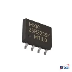
圖片僅供參考
LT1308AIS8
+物料清單Switching Voltage Regulators LT1308A and B - Single Cell High Current Micropower 600kHz Boost DC/DC Converter
-
製造商類比設備
-
製造商部分 #LT1308AIS8
-
有存貨15326
365 天品質保證
7*24 小時服務保證
90-日售後保障
正品保證
規格
| 屬性 | 價值 |
概述
Description
The LT1308AIS8 is a DC/DC step-up converter integrated circuit designed by Analog Devices, also known by its linear technology brand. It is particularly suited for applications requiring high efficiency in converting low voltages to higher output levels, such as in battery-powered devices. The device operates with a wide input voltage range and can deliver high output currents, making it versatile for various applications.
Key features include a low quiescent current, which helps conserve battery life, and a high switching frequency, allowing the use of smaller external components, thus reducing the overall size of the application circuit. The LT1308AIS8 also includes internal power MOSFETs, further simplifying the design by minimizing the need for external components.
It is typically used in portable devices, where efficiency and compactness are crucial, such as in mobile phones, handheld instruments, and other consumer electronics. Additionally, the device's design ensures robust performance with minimal electromagnetic interference, an essential factor in maintaining signal integrity in sensitive applications.
Key features include a low quiescent current, which helps conserve battery life, and a high switching frequency, allowing the use of smaller external components, thus reducing the overall size of the application circuit. The LT1308AIS8 also includes internal power MOSFETs, further simplifying the design by minimizing the need for external components.
It is typically used in portable devices, where efficiency and compactness are crucial, such as in mobile phones, handheld instruments, and other consumer electronics. Additionally, the device's design ensures robust performance with minimal electromagnetic interference, an essential factor in maintaining signal integrity in sensitive applications.
Equivalent
The LT1308AIS8 is a MicroPower step-up DC/DC converter. Equivalent products could include:
1. MAX856 from Maxim Integrated.
2. TPS61070 from Texas Instruments.
3. NCP1400 from ON Semiconductor.
4. MCP1640 from Microchip Technology.
Ensure to check the specific electrical and pin compatibility before considering a replacement, as these might differ slightly in specs or require different configurations.
1. MAX856 from Maxim Integrated.
2. TPS61070 from Texas Instruments.
3. NCP1400 from ON Semiconductor.
4. MCP1640 from Microchip Technology.
Ensure to check the specific electrical and pin compatibility before considering a replacement, as these might differ slightly in specs or require different configurations.
Features
The LT1308AIS8 is a micropower DC/DC step-up converter designed for battery-powered applications. It is notable for its high efficiency and the ability to operate at low input voltages. Key features include:
1. Input Voltage Range: It operates with an input voltage as low as 1V, making it suitable for applications with single-cell battery inputs.
2. Output Voltage: The device can be configured to provide output voltages up to 12V.
3. Efficiency: Designed for high efficiency, often exceeding 90%, which is critical in battery-powered devices to extend battery life.
4. Current Capability: It can deliver up to 1A of output current, depending on the input voltage and output voltage settings.
5. Low Quiescent Current: The device features a low quiescent current, which helps in reducing power consumption when the device is idle.
6. PWM Control: It uses pulse-width modulation (PWM) for stable operation across various load conditions.
7. Compact Package: Available in an 8-pin SOIC package, making it suitable for compact designs.
Overall, the LT1308AIS8 is ideal for portable, battery-operated devices requiring efficient voltage conversion.
1. Input Voltage Range: It operates with an input voltage as low as 1V, making it suitable for applications with single-cell battery inputs.
2. Output Voltage: The device can be configured to provide output voltages up to 12V.
3. Efficiency: Designed for high efficiency, often exceeding 90%, which is critical in battery-powered devices to extend battery life.
4. Current Capability: It can deliver up to 1A of output current, depending on the input voltage and output voltage settings.
5. Low Quiescent Current: The device features a low quiescent current, which helps in reducing power consumption when the device is idle.
6. PWM Control: It uses pulse-width modulation (PWM) for stable operation across various load conditions.
7. Compact Package: Available in an 8-pin SOIC package, making it suitable for compact designs.
Overall, the LT1308AIS8 is ideal for portable, battery-operated devices requiring efficient voltage conversion.
Pinout
The LT1308AIS8 is a micropower, high-efficiency DC/DC converter designed by Linear Technology (now part of Analog Devices). It is typically used for boosting low voltage inputs to higher output voltages. The LT1308AIS8 comes in an 8-pin SOIC (Small Outline Integrated Circuit) package.
The functions of the pins are as follows:
1. SW (Pin 1): Switch Pin. Connects to the inductor and is the point where the switching action takes place.
2. GND (Pin 2): Ground. Common reference point for the circuit.
3. FB (Pin 3): Feedback Pin. Used to set the output voltage via a resistor divider network.
4. SHDN (Pin 4): Shutdown Pin. A low signal on this pin turns off the converter.
5. VINA (Pin 5): Input Voltage for Analog Circuits. Powers the control circuitry.
6. VIN (Pin 6): Input Supply Pin. Connects to the input voltage source.
7. VOUT (Pin 7): Output Voltage Sense Pin. Used for output voltage sensing.
8. SW (Pin 8): Another Switch Pin, typically connected to the same inductor as Pin 1.
This configuration allows for efficient step-up voltage conversion suitable for battery-powered applications.
The functions of the pins are as follows:
1. SW (Pin 1): Switch Pin. Connects to the inductor and is the point where the switching action takes place.
2. GND (Pin 2): Ground. Common reference point for the circuit.
3. FB (Pin 3): Feedback Pin. Used to set the output voltage via a resistor divider network.
4. SHDN (Pin 4): Shutdown Pin. A low signal on this pin turns off the converter.
5. VINA (Pin 5): Input Voltage for Analog Circuits. Powers the control circuitry.
6. VIN (Pin 6): Input Supply Pin. Connects to the input voltage source.
7. VOUT (Pin 7): Output Voltage Sense Pin. Used for output voltage sensing.
8. SW (Pin 8): Another Switch Pin, typically connected to the same inductor as Pin 1.
This configuration allows for efficient step-up voltage conversion suitable for battery-powered applications.
Manufacturer
The LT1308AIS8 is manufactured by Analog Devices, Inc. Analog Devices is a multinational semiconductor company specializing in the design and manufacturing of analog, mixed-signal, and digital signal processing integrated circuits. These products are used in a wide variety of electronic equipment and applications, including telecommunications, industrial automation, automotive systems, healthcare devices, and consumer electronics. The company is known for its innovation in the field of semiconductors and provides solutions that bridge the physical and digital worlds.
Application
The LT1308AIS8 is a high-efficiency, step-up DC/DC converter commonly used in applications requiring low power consumption and compact size. Its application areas include:
1. Portable Devices: Ideal for powering mobile phones, PDAs, and handheld instruments due to its efficiency in boosting battery voltage.
2. Battery-Powered Equipment: Suitable for devices needing efficient power conversion from lower battery voltages.
3. LCD Bias Supplies: Used in generating higher voltages required by LCD screens in portable electronics.
4. Power Management: Employed in systems requiring efficient battery power management and conversion.
5. Consumer Electronics: Useful in a variety of gadgets where space-saving and energy efficiency are crucial.
These applications leverage the LT1308AIS8's ability to deliver high efficiency and compact form factor.
1. Portable Devices: Ideal for powering mobile phones, PDAs, and handheld instruments due to its efficiency in boosting battery voltage.
2. Battery-Powered Equipment: Suitable for devices needing efficient power conversion from lower battery voltages.
3. LCD Bias Supplies: Used in generating higher voltages required by LCD screens in portable electronics.
4. Power Management: Employed in systems requiring efficient battery power management and conversion.
5. Consumer Electronics: Useful in a variety of gadgets where space-saving and energy efficiency are crucial.
These applications leverage the LT1308AIS8's ability to deliver high efficiency and compact form factor.
Package
The LT1308AIS8 is housed in an 8-lead SOIC (Small Outline Integrated Circuit) package.