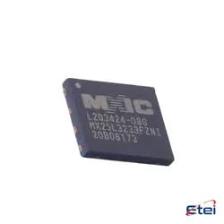
規格
| 屬性 | 價值 |
| Package | Tray |
| Series | ECP3 |
| ProductStatus | Active |
| NumberofLABs/CLBs | 8375 |
| NumberofLogicElements/Cells | 67000 |
| TotalRAMBits | 4526080 |
| NumberofI/O | 380 |
| Voltage-Supply | 1.14V ~ 1.26V |
| MountingType | Surface Mount |
| OperatingTemperature | 0°C ~ 85°C (TJ) |
| Package/Case | 672-BBGA |
概述
Description
The LFE3-70EA-8FN672C is a member of the LatticeECP3 FPGA family, specifically designed to deliver optimal performance and low power consumption for a broad range of applications, including communications, consumer electronics, and industrial systems. It features 70,000 LUTs (Look-Up Tables), which makes it suitable for handling complex processing tasks.
This FPGA is built on a 65nm low-power process technology, ensuring efficient power usage. It supports high-speed I/Os and protocols like PCI Express, Ethernet, and CPRI/OBSAI, making it versatile for networking and signal processing tasks. The "-8" in its part number indicates its speed grade, which is a measure of its performance level, with lower numbers generally indicating higher speed capabilities.
The package type, "FN672," refers to a Fine-Pitch Ball Grid Array (FBGA) with 672 pins, aiding in compact and efficient board designs. The "C" denotes the commercial temperature range, meaning it is suitable for standard operating environments. Overall, the LFE3-70EA-8FN672C offers a balanced mix of performance, power efficiency, and connectivity options.
This FPGA is built on a 65nm low-power process technology, ensuring efficient power usage. It supports high-speed I/Os and protocols like PCI Express, Ethernet, and CPRI/OBSAI, making it versatile for networking and signal processing tasks. The "-8" in its part number indicates its speed grade, which is a measure of its performance level, with lower numbers generally indicating higher speed capabilities.
The package type, "FN672," refers to a Fine-Pitch Ball Grid Array (FBGA) with 672 pins, aiding in compact and efficient board designs. The "C" denotes the commercial temperature range, meaning it is suitable for standard operating environments. Overall, the LFE3-70EA-8FN672C offers a balanced mix of performance, power efficiency, and connectivity options.
Equivalent
The Lattice LFE3-70EA-8FN672C is part of the ECP3 FPGA family. Equivalent products from other manufacturers include:
1. Xilinx Spartan-6 series, such as XC6SLX75.
2. Intel (Altera) Cyclone IV series, such as EP4CE75.
These products have comparable logic elements, I/O capabilities, and similar applications in cost-sensitive, high-volume applications requiring moderate performance. Always check specific requirements like power consumption and package type to ensure compatibility.
1. Xilinx Spartan-6 series, such as XC6SLX75.
2. Intel (Altera) Cyclone IV series, such as EP4CE75.
These products have comparable logic elements, I/O capabilities, and similar applications in cost-sensitive, high-volume applications requiring moderate performance. Always check specific requirements like power consumption and package type to ensure compatibility.
Features
The LFE3-70EA-8FN672C is a member of the LatticeECP3 FPGA family. Key features include:
1. Logic Capacity: It has approximately 70,000 LUTs, which provides substantial logic for complex designs.
2. Low Power: Designed for low power consumption, suitable for power-sensitive applications.
3. Embedded Memory: Includes embedded block RAM to facilitate data storage and retrieval.
4. DSP Blocks: Contains dedicated DSP blocks for efficient signal processing tasks.
5. I/O Features: Supports a wide range of I/O standards and includes high-speed SERDES (Serializer/Deserializer) for data transmission.
6. Package: Comes in a 672-ball Fine Pitch Ball Grid Array (FPBGA) package.
7. Speed Grade: The "-8" indicates the speed grade, with higher numbers typically representing faster performance.
Overall, the LFE3-70EA-8FN672C is designed for applications requiring a balance of performance, power efficiency, and cost-effectiveness, such as communication systems, video processing, and industrial control systems.
1. Logic Capacity: It has approximately 70,000 LUTs, which provides substantial logic for complex designs.
2. Low Power: Designed for low power consumption, suitable for power-sensitive applications.
3. Embedded Memory: Includes embedded block RAM to facilitate data storage and retrieval.
4. DSP Blocks: Contains dedicated DSP blocks for efficient signal processing tasks.
5. I/O Features: Supports a wide range of I/O standards and includes high-speed SERDES (Serializer/Deserializer) for data transmission.
6. Package: Comes in a 672-ball Fine Pitch Ball Grid Array (FPBGA) package.
7. Speed Grade: The "-8" indicates the speed grade, with higher numbers typically representing faster performance.
Overall, the LFE3-70EA-8FN672C is designed for applications requiring a balance of performance, power efficiency, and cost-effectiveness, such as communication systems, video processing, and industrial control systems.
Pinout
The LFE3-70EA-8FN672C is part of the LatticeECP3 family of FPGAs. This particular model comes in a 672-ball Fine-Pitch Ball Grid Array (FPBGA) package. Therefore, it has a pin count of 672. These pins are used for various functions, including:
1. I/O Pins: For interfacing with external components, supporting various I/O standards.
2. Power and Ground Pins: To supply power and establish ground connections for the FPGA's operation.
3. Configuration Pins: Used during the programming and configuration of the FPGA.
4. Clock Pins: For clock input and distribution within the FPGA.
5. Dedicated Function Pins: These may include pins for special functionalities such as JTAG for testing and debugging.
The specific functions assigned to each pin can vary depending on the configuration and application requirements, and detailed information can typically be found in the device's datasheet or technical reference manual provided by Lattice Semiconductor.
1. I/O Pins: For interfacing with external components, supporting various I/O standards.
2. Power and Ground Pins: To supply power and establish ground connections for the FPGA's operation.
3. Configuration Pins: Used during the programming and configuration of the FPGA.
4. Clock Pins: For clock input and distribution within the FPGA.
5. Dedicated Function Pins: These may include pins for special functionalities such as JTAG for testing and debugging.
The specific functions assigned to each pin can vary depending on the configuration and application requirements, and detailed information can typically be found in the device's datasheet or technical reference manual provided by Lattice Semiconductor.
Manufacturer
The LFE3-70EA-8FN672C is manufactured by Lattice Semiconductor. Lattice Semiconductor is a company that specializes in the design and production of low-power, field-programmable gate arrays (FPGAs) and related software and intellectual property. They focus on providing programmable logic solutions that are used in a wide range of applications, including communications, computing, consumer electronics, industrial, and automotive markets. The company's products are designed to be power-efficient and are used in devices where space, power consumption, and cost are critical factors.
Application
The LFE3-70EA-8FN672C is a member of the LatticeECP3 FPGA family, which is known for low power consumption and cost-effectiveness. Key application areas include:
1. Telecommunications: Used in base stations, wireless infrastructure, and high-speed networking equipment.
2. Industrial Automation: Supports motor control, industrial networking, and surveillance systems.
3. Medical Devices: Implements imaging systems and diagnostic tools.
4. Consumer Electronics: Utilized in HD displays and digital cameras.
5. Aerospace and Defense: Deployed for secure communications and signal processing.
These applications leverage the FPGA's high-speed SERDES, DSP capabilities, and low-power architecture.
1. Telecommunications: Used in base stations, wireless infrastructure, and high-speed networking equipment.
2. Industrial Automation: Supports motor control, industrial networking, and surveillance systems.
3. Medical Devices: Implements imaging systems and diagnostic tools.
4. Consumer Electronics: Utilized in HD displays and digital cameras.
5. Aerospace and Defense: Deployed for secure communications and signal processing.
These applications leverage the FPGA's high-speed SERDES, DSP capabilities, and low-power architecture.
Package
The LFE3-70EA-8FN672C is a Field-Programmable Gate Array (FPGA) from the LatticeECP3 family. It comes in a Fine-Pitch Ball Grid Array (FBGA) package with 672 pins.