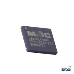
圖片僅供參考
JS28F640J3F75B
+物料清單NOR Flash Use JS28F640J3F75A
-
製造商聯盟記憶
-
製造商部分 #JS28F640J3F75B
-
有存貨23708
365 天品質保證
7*24 小時服務保證
90-日售後保障
正品保證
規格
| 屬性 | 價值 |
| Packaging | Reel |
| Standard Pack Qty | 1600 |
概述
Description
The JS28F640J3F75B is a model of Intel's StrataFlash memory product line. It is a 64 Mb (megabit) flash memory chip designed for high-performance, high-density storage applications. The chip utilizes Intel’s advanced flash technology, which allows for faster read and write operations compared to traditional flash memory. It operates with a voltage range of 1.8V to 3.6V, making it suitable for a wide array of electronic devices that require efficient power consumption.
Key features include block locking (which provides data protection), fast read access time, and a common flash interface (CFI) that ensures compatibility with various systems. Additionally, the chip supports execute-in-place (XIP), allowing programs to run directly from the flash memory, thereby enhancing device performance.
The JS28F640J3F75B is commonly used in consumer electronics, telecommunications, automotive, and industrial applications where reliable, non-volatile storage is crucial. Its architecture provides robust data retention and endurance, making it a versatile option for embedded system designs.
Key features include block locking (which provides data protection), fast read access time, and a common flash interface (CFI) that ensures compatibility with various systems. Additionally, the chip supports execute-in-place (XIP), allowing programs to run directly from the flash memory, thereby enhancing device performance.
The JS28F640J3F75B is commonly used in consumer electronics, telecommunications, automotive, and industrial applications where reliable, non-volatile storage is crucial. Its architecture provides robust data retention and endurance, making it a versatile option for embedded system designs.
Equivalent
The JS28F640J3F75B is a 64Mb NOR Flash Memory chip from Intel's StrataFlash Embedded Memory series. Equivalent products may include those from other manufacturers with similar specifications, such as the Micron MT28F640J3, Spansion (now part of Cypress Semiconductor) S29GL064N, and Macronix MX29LV640. These equivalents should offer similar storage capacity, interface, and performance characteristics. Always verify compatibility through datasheets and manufacturer specifications before substituting components.
Features
The JS28F640J3F75B is a flash memory component from Intel's StrataFlash® Embedded Memory family. Key features include:
1. Memory Capacity: It offers a 64 Megabit (Mb) capacity.
2. Architecture: Uniform 128 Kbyte block architecture, allowing for easier software management.
3. Voltage: Operates at a 3.3V supply voltage, which is typical for low-power applications.
4. Performance: Offers fast read and write performance with support for burst read mode.
5. Command Set: Utilizes an industry-standard command set that simplifies integration into existing systems.
6. Wear Leveling: Built-in mechanisms to extend the lifecycle through even distribution of write and erase cycles.
7. Security: Features hardware protection to prevent accidental write or erase operations.
8. Package: Available in various packages, including TSOP or BGA, accommodating different design requirements.
9. Operating Temperature: Designed to operate efficiently across a wide temperature range suitable for industrial applications.
These features make the JS28F640J3F75B suitable for embedded systems that demand reliable non-volatile memory storage.
1. Memory Capacity: It offers a 64 Megabit (Mb) capacity.
2. Architecture: Uniform 128 Kbyte block architecture, allowing for easier software management.
3. Voltage: Operates at a 3.3V supply voltage, which is typical for low-power applications.
4. Performance: Offers fast read and write performance with support for burst read mode.
5. Command Set: Utilizes an industry-standard command set that simplifies integration into existing systems.
6. Wear Leveling: Built-in mechanisms to extend the lifecycle through even distribution of write and erase cycles.
7. Security: Features hardware protection to prevent accidental write or erase operations.
8. Package: Available in various packages, including TSOP or BGA, accommodating different design requirements.
9. Operating Temperature: Designed to operate efficiently across a wide temperature range suitable for industrial applications.
These features make the JS28F640J3F75B suitable for embedded systems that demand reliable non-volatile memory storage.
Pinout
The JS28F640J3F75B is part of Intel's StrataFlash® Memory family. It is a 64 Mbit (8 MB) flash memory device. The chip typically comes in a 56-lead TSOP (Thin Small Outline Package) or a 64-ball Easy BGA (Ball Grid Array) package.
Pin Count:
- TSOP Package: 56 pins
- Easy BGA Package: 64 balls
Key Functions:
- Address Pins (A0-A21): Used to select the memory location.
- Data Pins (DQ0-DQ15): Used for data input/output.
- Control Pins: Include Chip Enable (CE#), Output Enable (OE#), and Write Enable (WE#) for controlling read and write operations.
- Reset/Power-Down (RP#): Used to reset the device or put it into power-down mode.
- Write Protect (WP#): Protects the highest address block from being written to.
- Status Indicator: Provides information about the status of the device (Ready/Busy).
Additional pins may include power and ground connections, as well as other control or specific function pins that support the operational characteristics of the flash memory.
Pin Count:
- TSOP Package: 56 pins
- Easy BGA Package: 64 balls
Key Functions:
- Address Pins (A0-A21): Used to select the memory location.
- Data Pins (DQ0-DQ15): Used for data input/output.
- Control Pins: Include Chip Enable (CE#), Output Enable (OE#), and Write Enable (WE#) for controlling read and write operations.
- Reset/Power-Down (RP#): Used to reset the device or put it into power-down mode.
- Write Protect (WP#): Protects the highest address block from being written to.
- Status Indicator: Provides information about the status of the device (Ready/Busy).
Additional pins may include power and ground connections, as well as other control or specific function pins that support the operational characteristics of the flash memory.
Manufacturer
The JS28F640J3F75B is a flash memory chip manufactured by Intel Corporation. Intel is a multinational corporation and technology company headquartered in Santa Clara, California. It is one of the world's largest and highest-valued semiconductor chip manufacturers. Intel is renowned for its role in developing microprocessors, which are integral components of most personal computers. The company also produces other hardware components, including flash memory, integrated graphics, and networking products. Intel is known for its innovations in technology and its contributions to the advancement of computer processing power and efficiency.
Application
The JS28F640J3F75B is a NOR Flash memory device commonly used in various embedded systems and applications that require non-volatile storage. Its application areas include:
1. Consumer Electronics: Used in devices like digital cameras and audio players for firmware storage.
2. Industrial Systems: Employed in control systems and data logging where reliability is key.
3. Automotive: Utilized in infotainment systems and engine control units.
4. Networking Equipment: Used for storing firmware in routers and switches.
5. Telecommunications: Provides memory solutions for base stations and communication devices.
Its robust performance in sustaining read and write cycles makes it suitable for applications demanding high reliability.
1. Consumer Electronics: Used in devices like digital cameras and audio players for firmware storage.
2. Industrial Systems: Employed in control systems and data logging where reliability is key.
3. Automotive: Utilized in infotainment systems and engine control units.
4. Networking Equipment: Used for storing firmware in routers and switches.
5. Telecommunications: Provides memory solutions for base stations and communication devices.
Its robust performance in sustaining read and write cycles makes it suitable for applications demanding high reliability.
Package
The JS28F640J3F75B is a NOR Flash memory chip from Intel, typically found in a TSOP (Thin Small Outline Package). This package type is compact and suitable for surface mounting on PCBs, used in various applications requiring non-volatile storage.