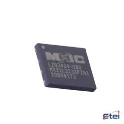
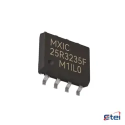
圖片僅供參考
AS4C256M16D4-75BCN
+物料清單IC DRAM 4GBIT PARALLEL 96FBGA
-
製造商Alliance Memory,股份有限公司。
-
製造商部分 #AS4C256M16D4-75BCN
-
有存貨8876
365 天品質保證
7*24 小時服務保證
90-日售後保障
正品保證
規格
| 屬性 | 價值 |
| Part Status | Not For New Designs |
| Digi Key Programmable | Not Verified |
| Memory Type | Volatile |
| Memory Format | DRAM |
| Technology | SDRAM - DDR4 |
| Memory Size | 4Gbit |
| Memory Organization | 256M x 16 |
| Memory Interface | Parallel |
| Write Cycle Time - Word, Page | 15ns |
| Voltage - Supply | 1.14V ~ 1.26V |
| Operating Temperature | 0°C ~ 95°C (TC) |
| Mounting Type | Surface Mount |
| Package / Case | 96-TFBGA |
| Supplier Device Package | 96-FBGA (7.5x13.5) |
| Base Product Number | AS4C256 |
| Clock Frequency | 1.333 GHz |
| Access Time | 18 ns |
概述
Description
The AS4C256M16D4-75BCN is a high-performance DRAM (Dynamic Random-Access Memory) module manufactured by Alliance Memory. This specific model is organized as 256M x 16 and is based on DDR3 SDRAM technology, which is known for its high speed and efficiency. The "75BCN" in its designation typically refers to the speed and packaging, with "75" indicating a cycle time of 7.5 nanoseconds, making it suitable for applications requiring fast data processing.
This memory chip is commonly used in a variety of electronic products, including computers, networking equipment, and consumer electronics, due to its reliable performance and compatibility with a broad range of systems. The AS4C256M16D4-75BCN supports robust data integrity and error correction mechanisms, making it ideal for environments where data accuracy is critical. Its compact design and low power consumption also contribute to its appeal for portable and energy-efficient devices. Overall, it serves as a versatile and dependable memory solution in both industrial and consumer applications.
This memory chip is commonly used in a variety of electronic products, including computers, networking equipment, and consumer electronics, due to its reliable performance and compatibility with a broad range of systems. The AS4C256M16D4-75BCN supports robust data integrity and error correction mechanisms, making it ideal for environments where data accuracy is critical. Its compact design and low power consumption also contribute to its appeal for portable and energy-efficient devices. Overall, it serves as a versatile and dependable memory solution in both industrial and consumer applications.
Equivalent
The AS4C256M16D4-75BCN is a 4Gb DDR3L SDRAM chip. Equivalent products include:
1. Micron MT41K256M16TW-107 IT:P
2. Samsung K4B4G1646D-BYK0
3. SK Hynix H5TC4G63AFR-PBA
4. Nanya NT5CB256M16BP-DI
These chips share similar specifications in terms of capacity, voltage requirements, and speed, making them suitable alternatives in various applications.
1. Micron MT41K256M16TW-107 IT:P
2. Samsung K4B4G1646D-BYK0
3. SK Hynix H5TC4G63AFR-PBA
4. Nanya NT5CB256M16BP-DI
These chips share similar specifications in terms of capacity, voltage requirements, and speed, making them suitable alternatives in various applications.
Pinout
The AS4C256M16D4-75BCN is a 4Gb DDR4 SDRAM chip organized as 256M x 16 bits. It typically comes in a 96-ball FBGA (Fine-Pitch Ball Grid Array) package, although specific pin counts may vary slightly depending on the exact configuration and manufacturer specifications. The primary functions of the pins include:
1. Power Supply and Ground: Pins for VDD, VDDQ (power supply for the memory core and I/O), and VSS (ground).
2. Data and Data Mask: Data lines (DQ) and data mask (DM) for read/write operations.
3. Address and Control Signals: Address lines (A0-A15, etc.) and bank address lines (BA0, BA1, etc.) used for accessing memory locations.
4. Command Signals: Command inputs like WE# (Write Enable), CAS# (Column Address Strobe), and RAS# (Row Address Strobe) for executing operations.
5. Clock Signals: Differential clock inputs (CK, CK#) for synchronizing operations.
6. Other Functions: CKE (Clock Enable), ODT (On-Die Termination), and RESET# for additional control functions.
For precise pin count and detailed functional pin descriptions, consulting the specific datasheet from the manufacturer is recommended.
1. Power Supply and Ground: Pins for VDD, VDDQ (power supply for the memory core and I/O), and VSS (ground).
2. Data and Data Mask: Data lines (DQ) and data mask (DM) for read/write operations.
3. Address and Control Signals: Address lines (A0-A15, etc.) and bank address lines (BA0, BA1, etc.) used for accessing memory locations.
4. Command Signals: Command inputs like WE# (Write Enable), CAS# (Column Address Strobe), and RAS# (Row Address Strobe) for executing operations.
5. Clock Signals: Differential clock inputs (CK, CK#) for synchronizing operations.
6. Other Functions: CKE (Clock Enable), ODT (On-Die Termination), and RESET# for additional control functions.
For precise pin count and detailed functional pin descriptions, consulting the specific datasheet from the manufacturer is recommended.
Manufacturer
The manufacturer of the AS4C256M16D4-75BCN is Alliance Memory, Inc. Alliance Memory is a company that specializes in the production and supply of legacy memory products, including SRAM, DRAM, and SDRAM. They focus on supporting customers with stable and reliable memory solutions, particularly for older systems and applications that require specific memory types no longer widely available from other manufacturers. Alliance Memory targets industries such as telecommunications, medical, automotive, and industrial electronics, where long product life cycles and consistency are crucial.
Application
The AS4C256M16D4-75BCN is a DRAM chip used in various applications that require high-speed data processing and storage. Common application areas include:
1. Consumer Electronics: Used in devices like TVs and gaming consoles to manage memory-intensive tasks.
2. Computing: Integrated into laptops and desktops for efficient data handling.
3. Networking Equipment: Supports routers and switches for managing data traffic.
4. Telecommunications: Contributes to communication systems requiring robust data management.
5. Industrial Systems: Utilized in automation and control systems for efficient processing.
6. Embedded Systems: Powers devices with embedded applications, such as IoT devices.
These applications benefit from the chip's ability to handle large volumes of data quickly and reliably.
1. Consumer Electronics: Used in devices like TVs and gaming consoles to manage memory-intensive tasks.
2. Computing: Integrated into laptops and desktops for efficient data handling.
3. Networking Equipment: Supports routers and switches for managing data traffic.
4. Telecommunications: Contributes to communication systems requiring robust data management.
5. Industrial Systems: Utilized in automation and control systems for efficient processing.
6. Embedded Systems: Powers devices with embedded applications, such as IoT devices.
These applications benefit from the chip's ability to handle large volumes of data quickly and reliably.
Package
The AS4C256M16D4-75BCN is a DDR3 SDRAM memory chip. Its package type is typically a 96-ball Fine-pitch Ball Grid Array (FBGA), which is common for DDR3 memory modules. This package offers a compact form factor, ideal for high-density memory applications.