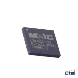
圖片僅供參考
AO6601
+物料清單MOSFET N/P-CH 30V 6-TSOP
-
製造商阿爾法歐米茄電晶體股份有限公司。
-
製造商部分 #AO6601
-
數據表 AO6601 DataSheet
-
包裹 SOT-457
-
有存貨2207
365 天品質保證
7*24 小時服務保證
90-日售後保障
正品保證
規格
| 屬性 | 價值 |
| Package / Case | Tape & Reel (TR) |
| Part Status | Active |
| FET Type | N and P-Channel Complementary |
| FET Feature | Logic Level Gate |
| Drain to Source Voltage (Vdss) | 30V |
| Current - Continuous Drain(Id) @ 25°C | 3.4A, 2.3A |
| Rds On(Max) @ Id Vgs | 60mOhm @ 3.4A, 10V |
| Vgs(th)(Max) @ Id | 1.5V @ 250µA |
| Gate Charge(Qg)(Max) @ Vgs | 12nC @ 10V |
| Input Capacitance(Ciss)(Max) @ Vds | 285pF @ 15V |
| Power - Max | 1.15W |
| Operating Temperature | -55°C ~ 150°C (TJ) |
| Mounting Type | Surface Mount |
概述
Description
Key specifications:
- Voltage Rating: 30V
- Current Rating: 6A per channel
- Low RDS(on): Typically 28mΩ (VGS = 10V)
- Logic-Level Gate Drive: Compatible with 5V/3.3V control signals
- Package: SOIC-8 or DFN (space-saving options)
Advantages include reduced power loss, compact footprint, and thermal efficiency. Common uses include battery protection, motor control, and voltage regulation. Always refer to the datasheet for detailed electrical characteristics and application guidelines.
Equivalent
- SiA416DJ (Vishay)
- DMN3010LSD (Diodes Inc.)
- FDS6898A (ON Semiconductor)
- IRLML6402 (Infineon)
These alternatives offer comparable specs (30V, 5.5A, low RDS(on)). Verify pin compatibility and electrical characteristics for your application.
Features
- Low On-Resistance (RDS(on)): Typically 28mΩ at VGS = 4.5V, reducing power loss.
- Low Gate Charge (Qg): Enhances switching efficiency.
- Compact Package: DFN3x3 (Dual Flat No-Lead) for space-saving designs.
- Wide Voltage Range: Supports 20V drain-to-source voltage (VDS).
- High Current Handling: Up to 6.3A continuous drain current per channel.
- Logic-Level Gate Drive: Optimized for 2.5V to 4.5V gate-to-source voltage (VGS).
- Fast Switching: Suitable for high-frequency applications like DC-DC converters and power management.
Ideal for portable electronics, power supplies, and load switching.
Pinout
Pin Functions:
1. Pins 1, 2, 3 (Drain 1, Gate 1, Source 1): Control the first MOSFET.
2. Pins 5, 6, 7 (Drain 2, Gate 2, Source 2): Control the second MOSFET.
3. Pins 4, 8: No connection (NC) or thermal pad (varies by manufacturer).
Key Features:
- Low on-resistance (RDS(on)).
- High current handling (typically 6A per channel).
- Common in power switching and load control applications.
For exact details, refer to the datasheet.
Manufacturer
Application
1. Power Supplies – DC-DC converters, voltage regulation.
2. Battery Management – Protection circuits, discharge control.
3. Load Switching – Efficient power distribution in portable devices.
4. Motor Control – Driving small motors in consumer electronics.
5. LED Drivers – Current control in lighting systems.
Its low on-resistance and compact package make it ideal for space-constrained, high-efficiency designs.