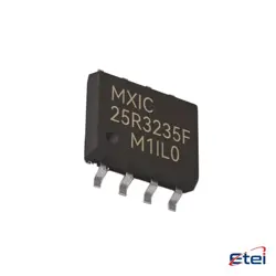
圖片僅供參考
74LVC1G157GV
+物料清單Encoders, Decoders, Multiplexers & Demultiplexers
-
製造商Nexperia
-
製造商部分 #74LVC1G157GV
-
有存貨29426
365 天品質保證
7*24 小時服務保證
90-日售後保障
正品保證
規格
| 屬性 | 價值 |
概述
Description
The 74LVC1G157GV is a single 2-input multiplexer designed for digital logic applications. It is a member of the 74LVC family, known for its low-voltage CMOS technology, which allows for high-speed signal processing while maintaining low power consumption. The device features a single data select input, two data inputs, and one output. It operates over a wide supply voltage range from 1.65V to 5.5V, making it versatile for various applications.
The 74LVC1G157GV is designed to route one of the two data inputs to the output based on the logic level of the select input. It supports a typical propagation delay of 4.8 ns at 3.3V, which ensures efficient data handling in high-speed circuits. The device is also equipped with features like input/output overvoltage tolerance and latch-up protection, enhancing its robustness in complex systems.
Packaged in a compact SOT353 or SC-74A, it is suitable for space-constrained designs. This multiplexer is commonly used in signal routing, data selection, and logic function implementation in electronic systems.
The 74LVC1G157GV is designed to route one of the two data inputs to the output based on the logic level of the select input. It supports a typical propagation delay of 4.8 ns at 3.3V, which ensures efficient data handling in high-speed circuits. The device is also equipped with features like input/output overvoltage tolerance and latch-up protection, enhancing its robustness in complex systems.
Packaged in a compact SOT353 or SC-74A, it is suitable for space-constrained designs. This multiplexer is commonly used in signal routing, data selection, and logic function implementation in electronic systems.
Equivalent
The 74LVC1G157GV is a single 2-input multiplexer in a small package. Equivalent products include:
1. Nexperia 74LVC1G157GW
2. Texas Instruments SN74LVC1G157DBVR
3. ON Semiconductor MC74VHC1G157DFT2G
4. Microchip Technology 74AHC1G157
These components have similar functions and electrical characteristics, with variations mainly in the packaging and environmental specifications. Always verify compatibility based on your specific application requirements.
1. Nexperia 74LVC1G157GW
2. Texas Instruments SN74LVC1G157DBVR
3. ON Semiconductor MC74VHC1G157DFT2G
4. Microchip Technology 74AHC1G157
These components have similar functions and electrical characteristics, with variations mainly in the packaging and environmental specifications. Always verify compatibility based on your specific application requirements.
Features
The 74LVC1G157GV is a single 2-to-1 multiplexer, which is part of the 74LVC family of logic devices. Key features include:
1. High-Speed Performance: It operates at a high-speed rate, making it suitable for applications that require fast data processing.
2. Low Power Consumption: It is designed to consume minimal power, which is ideal for portable and battery-powered devices.
3. Wide Operating Voltage Range: The device supports a broad supply voltage range from 1.65 V to 5.5 V, allowing for flexibility in various circuit designs.
4. 5V Tolerant Inputs: It can handle input signals up to 5 V, even when operating at a lower supply voltage, enhancing its compatibility with higher voltage systems.
5. Compact Package: The 74LVC1G157GV is available in a small SOT353 package, making it suitable for space-constrained applications.
6. Overvoltage Tolerant: The inputs are overvoltage tolerant, ensuring robustness against unexpected voltage surges.
7. Lead-Free and RoHS Compliant: It adheres to environmental and safety standards, being lead-free and compliant with the Restriction of Hazardous Substances Directive.
1. High-Speed Performance: It operates at a high-speed rate, making it suitable for applications that require fast data processing.
2. Low Power Consumption: It is designed to consume minimal power, which is ideal for portable and battery-powered devices.
3. Wide Operating Voltage Range: The device supports a broad supply voltage range from 1.65 V to 5.5 V, allowing for flexibility in various circuit designs.
4. 5V Tolerant Inputs: It can handle input signals up to 5 V, even when operating at a lower supply voltage, enhancing its compatibility with higher voltage systems.
5. Compact Package: The 74LVC1G157GV is available in a small SOT353 package, making it suitable for space-constrained applications.
6. Overvoltage Tolerant: The inputs are overvoltage tolerant, ensuring robustness against unexpected voltage surges.
7. Lead-Free and RoHS Compliant: It adheres to environmental and safety standards, being lead-free and compliant with the Restriction of Hazardous Substances Directive.
Pinout
The 74LVC1G157GV is a single 2-to-1 multiplexer. It has a total of 6 pins. The pin functions are as follows:
1. VCC: Power supply pin.
2. GND: Ground pin.
3. A: Data input pin A.
4. B: Data input pin B.
5. S: Select input pin to choose between inputs A and B.
6. Y: Output pin that provides the selected input.
This device allows you to select one of the two inputs and direct it to the output based on the logic level of the select pin (S). When S is low, the output Y reflects the state of input A, and when S is high, it reflects the state of input B. The 74LVC1G157GV is commonly used for data routing in digital circuits due to its low power consumption and high-speed performance.
1. VCC: Power supply pin.
2. GND: Ground pin.
3. A: Data input pin A.
4. B: Data input pin B.
5. S: Select input pin to choose between inputs A and B.
6. Y: Output pin that provides the selected input.
This device allows you to select one of the two inputs and direct it to the output based on the logic level of the select pin (S). When S is low, the output Y reflects the state of input A, and when S is high, it reflects the state of input B. The 74LVC1G157GV is commonly used for data routing in digital circuits due to its low power consumption and high-speed performance.
Manufacturer
The 74LVC1G157GV is manufactured by Nexperia. Nexperia is a global semiconductor company that specializes in producing discrete, logic, and MOSFET devices. Originally part of NXP Semiconductors, Nexperia became an independent company in 2017. The company focuses on creating high-quality, efficient, and reliable semiconductor components that are widely used in automotive, industrial, computing, and consumer electronics applications. Nexperia is known for its extensive portfolio of products that are essential for power management, signal conditioning, and other electronic functions.
Application
The 74LVC1G157GV is a single 2-to-1 multiplexer used in digital circuits. Its primary application areas include:
1. Data Routing: Used in digital systems to route signals or data from one of two sources to a single output.
2. Signal Selection: Selects between two data inputs for microprocessor or memory interfacing.
3. Logic Function Implementation: Used in implementing complex logic functions by combining with other logic gates.
4. Embedded Systems: Useful in resource-constrained environments for signal control and data management.
5. Communication Systems: Employed in systems requiring efficient data path control.
Its low power consumption and high-speed operation make it ideal for portable and high-speed applications.
1. Data Routing: Used in digital systems to route signals or data from one of two sources to a single output.
2. Signal Selection: Selects between two data inputs for microprocessor or memory interfacing.
3. Logic Function Implementation: Used in implementing complex logic functions by combining with other logic gates.
4. Embedded Systems: Useful in resource-constrained environments for signal control and data management.
5. Communication Systems: Employed in systems requiring efficient data path control.
Its low power consumption and high-speed operation make it ideal for portable and high-speed applications.
Package
The 74LVC1G157GV is a single 2-input multiplexer integrated circuit provided in a small SOT353 package, also known as a SC-70 or SC-88A package. This package type is compact, featuring a surface-mount design suitable for space-constrained applications.